
Electronic PCBs Facilitate Connectivity in Devices
Electrical signals are essential to the functioning of most electronic devices, but they won’t pass efficiently or reliably unless they have proper pathways. These conductive pathways, often made of copper, are the key to ensuring that signals reach their intended destinations. They also establish the framework for communication between components and between different layers of the board. The process of creating these pathways, known as etching, is the most critical step in PCB design.
Conductive pathways are created by chemically dividing the copper foil into separate conductive paths called tracks or circuit traces, pads for connection points called lands, and vias that allow connections between layers of the board. These features are etched into the insulating material of the substrate, resulting in an intricate network of lines that are fixed in place and insulated from each other. These pathways facilitate communications between various components and ensure that signals travel in a continuous path from one end of the circuit to the other.
Printed circuit boards, or PCBs, are the building blocks of electronic devices. Almost all modern equipment in the fields of electronics, manufacturing, and medical uses electronic pcb board to operate. This includes navigation tools and media equipment like TVs and DVD players that can’t work without them, as well as industrial equipment used in production.
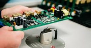
How Do Electronic PCBs Facilitate Connectivity in Devices?
PCBs are usually manufactured in a factory using a complex multi-step process that begins with the creation of a schematic diagram. The diagram is then translated to a layout on a blank copper-clad board by a computer program. The layout must take into account thermal considerations and geometry, as well as the placement of components and traces. Using automated electronic design automation software helps to reduce the time and effort required for this task.
The next step involves drilling holes through the pad areas of the board and then electroplating them with copper to form plated-through holes. These holes are then covered with a layer of solder mask, which prevents the solder from adhering to any conductive traces on the surface of the board. The bare board is then populated (or “stuffed”) with components.
This process can be performed by either through-hole or surface-mount technology. In through-hole technology the component leads plug into holes surrounded by conductive pads; the solder holds them in place. In surface-mount technology the component pins line up with conductive pads or lands on the pads, and the solder paste holds them in place during assembly.
The completed PCB is then given an optical inspection to verify that it matches the digital image generated from the original schematic diagram, and to check for any mistakes that may be difficult or impossible to correct afterwards. This is done with an automatic optical inspection machine that compares the digital image to the actual physical structure of the board. If the PCB is found to be incorrect, it’s discarded. Otherwise, the components and traces will be soldered to the board by hand.


