
Via in Pad
Via in pad is one of those things SMT guys like to frown upon, but with the right application it can be useful. Typically used for high-frequency circuits, via in pads can decrease trace length which reduces inductance and improve signal integrity. They can also be used for thermal control, placing a thermal via under heat-producing components to help sweep that heat away into copper layers or heat sinks on the PCB.
But a word of warning: it can be difficult to implement correctly, so we highly recommend working with an experienced contract PCB manufacturer that has successfully executed via in pad before. This will ensure that the proper drilling, filling, plating, and inspection processes are employed to avoid issues like solder wicking or voids.
In the world of PCBs, vias are tiny plated holes that connect copper tracks on different layers of the board. They’re an essential part of the circuit board manufacturing process, and there are many ways to use them in your design. For example, you can route small-pitch BGAs using the popular “dog bone” fanout pattern by transferring signals from the BGA footprint pad to a via, then from that via to other layers. Another use of vias is to place bypass capacitors close to the component, minimizing surface routing and parasitic inductance.
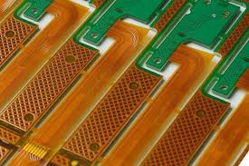
Via in Pad For High-Frequency Circuits
For high-speed designs, every millimeter counts. The shortest possible routing is critical to ensuring the integrity of a signal, and via in pads can minimize this path length by placing the capacitor directly under the component. It’s also a useful technique for tight spaces where the conventional fan out methods are not feasible, such as micro-BGA designs.
A downside to using via in pad is that it increases the cost of the board due to the extra processing required to manufacture the PCB with this method. The additional steps required to drill, fill, and plate the via can add up. In addition, there is a risk of voiding, solder wicking, or other defects that can lead to failure in the final product.
It’s important to understand the pros and cons of via in pad so that you can make a informed decision about whether or not it is appropriate for your design. Working closely with a trusted contract PCB manufacturer will help you determine if the advantages outweigh the risks and complexities of this advanced feature.
To minimize manufacturing costs, it’s best to use a conductive epoxy in the via rather than a non-conductive fill. This will ensure that the via is filled completely, and it will be much easier to apply solder paste accurately without wicking or voids. It’s important to also work with a manufacturer that can properly cap the via, which seals the opening and prevents it from leaking during assembly. This is accomplished by first filling the via with a conductive epoxy and then etching and plating the top of the via. This is an important step in reducing manufacturing defects and maximizing yield.


